- 您现在的位置:买卖IC网 > Sheet目录489 > NTHS5404T1G (ON Semiconductor)MOSFET N-CH 20V 5.2A CHIPFET
�� �
�
�NTHS5404T1�
�SOLDERING� FOOTPRINT*�
�1�
�2.03� 2�
�0.08�
�1�
�2.03� 2�
�0.08�
�1.72� 7�
�2.36� 2�
�0.093�
�0.63� 5�
�0.025�
�2.36� 2�
�0.093�
�0.068�
�PITCH�
�8X�
�0.45� 7�
�0.018�
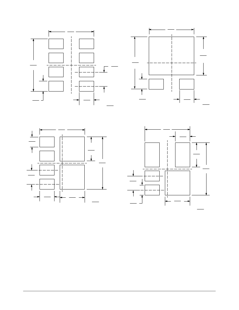
�Figure� 12.� Basic�
�8X�
�0.66�
�0.026�
�mm�
�inches�
�2X�
�0.45� 7�
�0.018�
�2X�
�0.66�
�0.026�
�Figure� 13.� Style� 1� and� 4�
�mm�
�inches�
�ADDITIONAL� SOLDERING� FOOTPRINTS*�
�1�
�2.03� 2�
�0.08�
�2.03� 2�
�0.08�
�2X�
�0.66�
�4X�
�0.45� 7�
�0.018�
�2X�
�1.09� 2�
�0.043�
�1�
�0.026�
�1.09� 2�
�0.043�
�2.36� 2�
�0.63� 5�
�0.025�
�PITC� H�
�0.093�
�0.63� 5�
�0.025�
�PITCH�
�2.36� 2�
�0.093�
�4X�
�0.66�
�0.026�
�Style� 2�
�2X�
�1.118�
�0.044�
�mm�
�inches�
�2X�
�0.45� 7�
�0.018�
�1.118�
�0.044�
�Style� 3�
�mm�
�inches�
�*For� additional� information� on� our� Pb� ?� Free� strategy� and� soldering�
�details,� please� download� the� ON� Semiconductor� Soldering� and�
�Mounting� Techniques� Reference� Manual,� SOLDERRM/D.�
�BASIC� PAD� PATTERNS�
�The� basic� pad� layout� with� dimensions� is� shown� in�
�Figure� 12.� This� is� sufficient� for� low� power� dissipation�
�MOSFET� applications,� but� power� semiconductor�
�performance� requires� a� greater� copper� pad� area,�
�particularly� for� the� drain� leads.�
�The� minimum� recommended� pad� pattern� shown� in�
�Figure� 13� improves� the� thermal� area� of� the� drain�
�confines� of� the� basic� footprint.� The� drain� copper� area� is�
�0.0054� sq.� in.� (or� 3.51� sq.� mm).� This� will� assist� the� power�
�dissipation� path� away� from� the� device� (through� the� copper�
�lead� ?� frame)� and� into� the� board� and� exterior� chassis� (if�
�applicable)� for� the� single� device.� The� addition� of� a� further�
�copper� area� and/or� the� addition� of� vias� to� other� board� layers�
�will� enhance� the� performance� still� further.�
�connections� (pins� 1,� 2,� 3,� 6,� 7,� 8)� while� remaining� within� the�
�http://onsemi.com�
�5�
�发布紧急采购,3分钟左右您将得到回复。
相关PDF资料
NTHS5441T1G
MOSFET PWR P-CH 3.9A 20V CHIPFET
NTHS5443T1
MOSFET P-CH 20V 3.6A CHIPFET
NTJD1155LT1
MOSFET/LOAD SWITCH HI 8V SOT-363
NTJD2152PT4G
MOSFET P-CH 8V DUAL ESD SOT-363
NTJD4001NT2G
MOSFET N-CH DUAL 30V SOT-363
NTJD4105CT2G
MOSFET N/P-CHAN COMPL SOT-363
NTJD4152PT1
MOSFET P-CHAN DUAL 20V SOT-363
NTJD4158CT1G
MOSFET N/P-CHAN COMPL SOT-363
相关代理商/技术参数
NTHS5404T1G
制造商:ON Semiconductor 功能描述:MOSFET
NTHS5441
制造商:ONSEMI 制造商全称:ON Semiconductor 功能描述:−20 V, −5.3 A, P−Channel ChipFET
NTHS5441PT1G
功能描述:MOSFET CHIPFETS 20V .055 TR PFET RoHS:否 制造商:STMicroelectronics 晶体管极性:N-Channel 汲极/源极击穿电压:650 V 闸/源击穿电压:25 V 漏极连续电流:130 A 电阻汲极/源极 RDS(导通):0.014 Ohms 配置:Single 最大工作温度: 安装风格:Through Hole 封装 / 箱体:Max247 封装:Tube
NTHS5441T1
功能描述:MOSFET -20V -5.3A P-Channel RoHS:否 制造商:STMicroelectronics 晶体管极性:N-Channel 汲极/源极击穿电压:650 V 闸/源击穿电压:25 V 漏极连续电流:130 A 电阻汲极/源极 RDS(导通):0.014 Ohms 配置:Single 最大工作温度: 安装风格:Through Hole 封装 / 箱体:Max247 封装:Tube
NTHS5441T1/D
制造商:未知厂家 制造商全称:未知厂家 功能描述:Power MOSFET P-Channel ChipFET
NTHS5441T1G
功能描述:MOSFET -20V -5.3A P-Channel RoHS:否 制造商:STMicroelectronics 晶体管极性:N-Channel 汲极/源极击穿电压:650 V 闸/源击穿电压:25 V 漏极连续电流:130 A 电阻汲极/源极 RDS(导通):0.014 Ohms 配置:Single 最大工作温度: 安装风格:Through Hole 封装 / 箱体:Max247 封装:Tube
NTHS5443
制造商:ONSEMI 制造商全称:ON Semiconductor 功能描述:Power MOSFET
NTHS5443T1
功能描述:MOSFET -20V -4.9A P-Channel RoHS:否 制造商:STMicroelectronics 晶体管极性:N-Channel 汲极/源极击穿电压:650 V 闸/源击穿电压:25 V 漏极连续电流:130 A 电阻汲极/源极 RDS(导通):0.014 Ohms 配置:Single 最大工作温度: 安装风格:Through Hole 封装 / 箱体:Max247 封装:Tube